 Mr. Chen:136-6225-2835
 Miss Chen:189-2385-0895
Shenzhen Guangjiayuan Electronic Technology Co., Ltd
Mr. Chen: 136-6225-2835 (same WeChat account)
QQ: 979285705
Miss Chen: 189-2385-0895 (same WeChat account)
QQ: 2391552662
Chen Weiting :135-3824-4786 (same WeChat account)
Chen Weihao: 139-2459-4393 (same WeChat account)
Tel: 86-0755-33182327
Email: gjydz88@163.com
Website: www.usb-type.com
Address: Building 10, Hongxing Gebu Qixiang, Songgang Town, Bao'an District, Shenzhen, Guangdong Province
1. The evolution history of the USB interface was in 1996, when the well-known Universal Serial Interface (USB) was first introduced. At that time, the USB interface in version 1.0 could only provide speeds of 1.5Mb/s and 12Mb/s in low speed (LS) mode and full speed (FS) mode, respectively. In 2000, USB 2.0 was launched. The new high-speed (HS) mode can provide a speed of up to 480Mb/s, and is still Backward compatibility with low-speed mode and full speed mode.
2. Overview of USB 3.0 System In November 2008, the USB 3.0 technical specifications were released. USB 3.0 not only includes all the features of USB 2.0 (HS, FS, and LS), but also provides a separate new ultra high speed data link called SuperSpeed. The ultra high speed link provides separate differential data lines for downloading (host=>device, referred to as the sending direction) and uploading in the receiving direction (device=>host). The maximum data rate provided by the ultra high speed mode is 5Gb/s (see Figure 1).
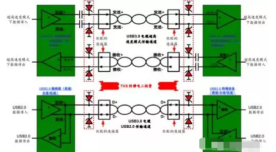
Figure 1: USB 3.0 ultra high speed mode and USB 2.0 mode physical links (achieving static protection on the host side and device side)
To support both USB 2.0 functionality and the new ultra high speed mode, the cable must adopt a new structure to provide three differential coupled signal lines (TX+/TX -, RX+/Rx -, and D+/D -). Vcc wires and grounding wires are also indispensable components in cables. The challenge faced by this low-cost USB 3.0 cable is to support high cutoff frequencies without interference between adjacent differential coupling pairs. (Please refer to Figure 2)
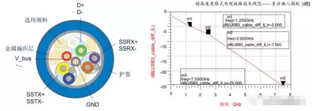
Figure 2 USB 3.0 Cable Structure and Cable Attenuation (Differential Mode)
In order to support all the lines included in the USB 3.0 cable, a new connector shape must be mandatory. The basic requirement of the new USB 3.0 connector is that it must be Backward compatibility with the USB 2.0 connector. From the perspective of electrostatic protection, this makes the ultra-high speed mode lines of the standard A connector easy to be hit by static electricity (on the host side and device side). A powerful strategy is to implement an efficient electrostatic protection mechanism in the USB 3.0 link.
One of the most serious problems faced by ultra-high speed data transmission systems is to ensure a certain degree of Signal integrity at the receiver. High Signal integrity is very important to achieve a very low bit error rate (for example, for the USb3.0 super speed mode, the typical bit error rate is 1E-12). The eye diagram shows the characteristics of Signal integrity.
In a perfect system with infinite bandwidth, the eye map is completely open. In the actual system, the transmission and reception impedance (90 ohm differential impedance) and all parasitic capacitors at the transmitter and receiver limit the rise time/Fall time of the signal. These parasitic capacitors exist inside the USB 3.0 transceiver and/or outside the PCB. Unmatched PCB circuits, USB 3.0 connectors, or other parallel capacitors can cause external parasitic capacitance. Therefore, these additional parallel capacitors must be as small as possible. It is also necessary to consider the low-pass frequency response of the USB 3.0 cable (see Figure 2). In order to counteract the attenuation of high-frequency signals, dedicated equalizers can be used at the sending and receiving ends to adjust the signal.
These measures help to speed up the signals at the rising and falling edges, resulting in a more open eye diagram (i.e., higher Signal integrity) (see Figure 3).
To achieve proper Signal integrity performance, the capacitance of the TVS diode must be very low, but on the other hand, the TVS diode must provide high electrostatic protection capability.

Figure 3 Signal restoration at the sending end (3.5dB standard parameter) and linear equalizer at the receiving end (standard parameter)
Figure 4 shows the eye simulation of the entire USB 3.0 link (with a bit error rate of 1E6). In Figure 4 (left figure), the received signal is measured before being processed by the receiver equalizer. In the figure (right), the signal is measured after being processed by the receiver equalizer. The red inner contour line shows the degree of eye opening obtained by extrapolation with a bit error rate of 1E12. The red and purple contour lines are the valid values for compliance testing in the ultra high speed mode specified in the USB 3.0 technical specifications. Comparing two eye images, the effect of using an equalizer on the receiving end is obvious.
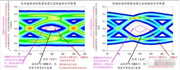
Figure 4 Signal eye diagram before receiving equalizer processing (left image) and signal eye diagram after receiving equalizer processing (right image)
The ultra-high speed link and the USB 2.0 transmission link use a differential coupled 90 ohm circuit. The signal reflection caused by the impedance mismatch inside the link will reduce Signal integrity. To avoid this situation, the entire layout design, including the USB 3.0 cable, should achieve 90 ohm differential impedance matching.
In order to minimize the "weakening slope" and provide the same line delay time, all differential coupling lines must be of the same length. This is particularly important for the USB 3.0 cable itself.
A high "weakening slope" will reduce Signal integrity, leading to the so-called "differential mode common mode signal conversion". The common mode signal produced will affect the smooth progress of EMI testing. An appropriate layout design for impedance matching can avoid these issues.
3、Design proposal for electrostatic protection layout of USB 3.0 ultra high speed link and USB 2.0 link
In the layout design of the entire USB 3.0 link, the following factors should be considered:
(1) All PCB circuits and interconnecting cables are mandatory to use a fully impedance matched 90 ohm differential design
(2) Non differential coupling lines must be minimized to the greatest extent possible. Non differential coupled circuits can seriously affect the degree of eye opening in eye maps
(3) The width and spacing of the 90 ohm differential coupled PCB circuit should not be too narrow to avoid additional losses, and these circuits should be sturdy enough for production. From a production perspective, the ideal line width for differential circuits is 0.3 millimeters and the line spacing is 0.2 millimeters. This will result in a dielectric height of 200 microns (assuming FR4 and er=4)
(4) The delay (line length) between the positive and negative lines of the differential coupling link (including the USB 3.0 cable) is exactly the same (minimizing the weakening slope). This is important for maintaining high Signal integrity and avoiding the generation of common mode signals.
Figure 5 shows an example of the cross-sectional layout design of a USB 3.0 standard A connector with both electrostatic protection circuits.
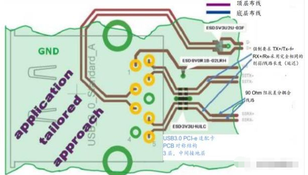
Figure 5 Layout design suggestions for standard A connector and Infineon electrostatic protection device USB 3.0
4、Modern Electrostatic Protection Strategy for USB 3.0
On the one hand, continuously reducing the size of each component of a chip is fundamental to reducing production costs and expanding working frequency. On the other hand, this miniaturization has also created new problems (for example, electrostatic breakdown is easy to occur). The demand for providing reliable electrostatic protection mechanisms is increasing day by day.
USb3.0 can provide a data rate of up to 5Gb/s, so the Fundamental frequency is up to 2.5GHz. In order to achieve high Signal integrity, the rise time and Fall time of the data signal must be very short. The treatment of the third or even fifth harmonic should not experience significant attenuation. This can only be achieved by utilizing cutting-edge semiconductor processes that minimize parasitic effects and have the fastest semiconductor switching speed. The disadvantage of this miniaturized semiconductor structure is that it is vulnerable to overvoltage caused by electrostatic discharge. Using built-in electrostatic protection devices can cause parasitic effects (parasitic capacitance) and occupy valuable on-chip space.
A very cost-effective approach is to combine the use of built-in electrostatic protection mechanisms (integrated into the USB 3.0 transceiver) with high-performance high current application circuits tailored to provide external electrostatic protection (implemented by device/circuit designers on circuit boards).
The built-in electrostatic protection mechanism is designed to provide device level protection only, for example, according to HBMJEDECJESD22-A115. The built-in electrostatic protection mechanism plays an important role in ensuring safe handling of devices during development, production, and circuit board assembly processes. The external TVS diode tailored specifically for this application achieves stricter system level protection in accordance with the IEC61000-4-2 standard.
In order to provide appropriate system level electrostatic protection for USB 3.0 links, electrostatic protection devices (TVS diodes) must meet different requirements. The electrostatic protection performance of TVS diodes can be determined based on the residual clamping voltage and the response of TVS diodes to specific electrostatic discharges, in accordance with the IEC61000-4-2 standard.
Some characteristics of TVS diodes can affect their electrostatic protection performance
Ÿ Lowest conduction resistance (R_on) (dynamic resistance (R_dynamic))
Ÿ The lowest breakdown voltage (V_Breakdown) is customized for this application
Based on experience, the clamping voltage (V_clamp) can be calculated:

Dynamic resistance can be derived based on the measured value of TLP (transmission line pulse). To ensure the safety of the application, the breakdown voltage must be consistent with the highest power supply voltage and highest signal level applied to the protected circuit (see Figure 6). The dynamic resistance (R_dyn) should be as small as possible. By combining the optimal breakdown voltage with the lowest dynamic resistance, the residual electrostatic discharge stress on the IC can be minimized to the greatest extent.
According to the TLP measurement chart, the dynamic resistance can be calculated (see Figure 6):
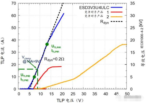
Figure 6 TLP measurement results of the Infineon ESD3V3U4UL tailored to provide electrostatic protection for USB3.0 ultra high speed links
To protect other USB 2.0 links, TVS diodes must provide slightly higher reverse operating voltage/breakdown voltage. To support both full speed and low speed modes, a higher breakdown voltage must be provided to form a signal amplitude of up to+5V. The Infineon ESD5V3U1U and ESD5V3U2U series can provide a minimum reverse operating voltage of 5.3V (breakdown voltage: minimum 6V) and a typical diode capacitance value of 0.4pF.
5. The Signal integrity of the USb3.0 ultra high speed link that has achieved electrostatic protection is simulated for the Signal integrity of the entire USb3.0 ultra high speed link when electrostatic protection is achieved and when electrostatic protection is not achieved. (Refer to Figure 1)
The entire transceiver area has a 90 ohm differential impedance. Considering the parasitic effects of the sender and receiver. The measured data indicates the status of the Usb3.0 cable. The maximum length of Usb3.0 cable is 3 meters.
In order to provide electrostatic protection for the USB 3.0 ultra high speed link, Infineon ESD3V3U4ULC is configured on both the host side and device side. ESD3V3U4ULC has excellent electrostatic protection performance and extremely low diode capacitance (diode to ground), with a typical value of 0.5pF. In the simulation, the basic layout design rules of the USB 3.0 ultra high speed link were considered. (Refer to Figure 5)
In the Signal integrity simulation of the entire USb3.0 ultra-high speed link, according to the USb3.0 compliance test standard parameters, the signal restoration at the sending end and the equalization processing at the receiving end are realized. Analyzed the eye pattern of the ultra-high speed signal processed by the receiver equalizer. The error rate used for simulation is 1E6. Based on the simulation results, the eye opening degree (red and blue contour lines) for a bit error rate of 1E12 is derived.
Calculate the degree of eye opening without TVS diode (red outline) and with TVS diode (ESD3V3U4ULC, blue outline), respectively. (Refer to Figure 7)
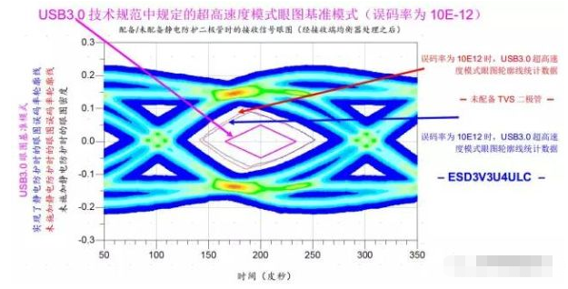
Figure 7 shows the eye view of ESD3V3U4ULC with and without ESD3V3U4ULC configuration on the host side and device side. The ultra-low capacitance TVS diode ESD3V3U4ULC is achieved on the host side and device side, and the degree of eye view opening (contour line) will be affected to some extent. Although the degree of eye opening may slightly decrease, it is still much larger than the benchmark mode (red purple outline) specified in the USB 3.0 technical specification.
The bathtub shaped curve simulation provides a detailed explanation of the role of TVS diodes. The black tick mark shows the voltage and time (picosecond) parameters of the eye pattern reference mode when the error rate specified in the USB 3.0 technical specification is 10E12. The red curve is calculated when TVS diodes are not equipped, and the blue curve is calculated when ESD3V3U4ULC is configured on the host side and device side.
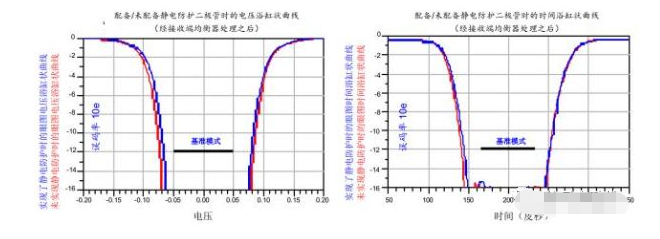
Figure 8 Simulation of voltage and time bathtub shaped curves with/without TVS diodes
6. Conclusion:
It is a mandatory requirement to carefully design the usb 3.0 interface to achieve the best system level electrostatic protection performance and Signal integrity. To meet both requirements, electrostatic protection devices must have excellent electrostatic protection performance and very low device capacitance. The Infineon ESD3V3U4ULC with an "array" configuration, coupled with a clear and clear layout design and high-quality links (USB 3.0 cables), can meet the above requirements.
Contact person:
Mr. Chen 136-6225-2835 (same WeChat account)
Miss Chen 189-2385-0895 (same WeChat account)
Chen Weiting 135-3824-4786 (same WeChat account)
Chen Weihao 139-2459-4393 (same WeChat account)
Address:
Building 10, Hongxing Gebu Qixiang, Songgang Town, Bao'an District, Shenzhen, Guangdong Province
 |
 |
| Technology 1 | Technology 2 |